➔ Index of ⦁ Linear Regulators ⦁
Linear regulators - Pass device
Going from an ideal model to a more realistic one: analysis of the pass device in linear regulators
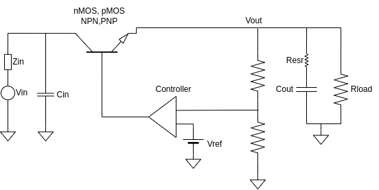
A realistic pass device
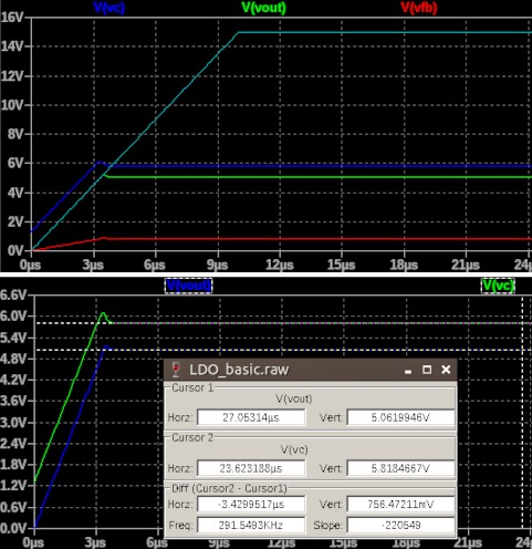
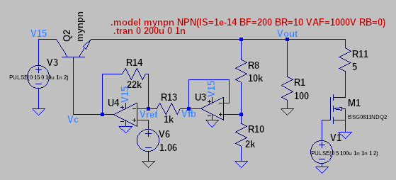
All the previous calculations have been made with an ideal NPN transistor but, as already said, some important parameters that have been neglected are the base resistance (in the previous chapter RB was set to 0Ohm in LTSpice simulation), the minority carriers transit time, internal parasitic capacitances. Now, if we substitute the pass device with a realistic NPN model - i.e. 2N2222 - we can see that its behaviour is different from the previous one. In the following you can find the circuit simulated and most relevant waveforms: for the NPN, first the provided ideal mynpn model was used, then it was substituted with the LTSpice 2N2222 model.
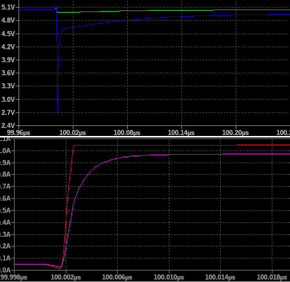
As you can see, the real BJT reacts very slowly to hard step loads so we need an output capacitor as a tank for such pulses. Moreover, we can see that the steady-state output voltage changes noticeably: this is because only a proportional term is present in the control loop, therefore a non-zero residual error will always be present. An integral term must be added, but this aspect will be covered later. The reason why we have such a high voltage drop with a real pass device is due to the slow reaction of a real BJT: between the base and emitter, there is a non-negligible capacitor, whose effect is visible when the base resistance is not zero. Moreover, the minority carrier transit time across the base is not zero (it was set to 0 by default in mynpn BJT model). Finally, the internal base resistance limits the base current during the step load (consider that during the step load, some current is provided to the emitter by the base rather than the collector). Let's look at a more accurate BJT model, accounting for internal parasitic parameters too. For now, let's use an ideal opamp for the feedback network, whose output current is not limited - a real opamp will limit its output current during the step load and has internal poles which can generate other dangerous instabilities or bad non-idealities.
BJT aspects involved in step load
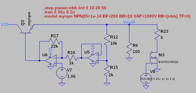
The BJT has two main parameters that affect the step load response: base resistance and transit time. We will focus on them trying to find a rule that can help us to get a better model, good for the step load response. Consider the following schematic as a reference for the simulations.
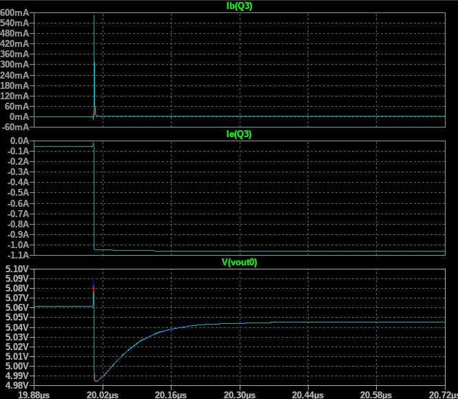
Variable base resistance with transit time set to 0s
Transit time set to 0s means that electrons flowing from emitter to collector need 0s to pass through the base This travel doesn't introduce any delay so every electron at the emitter is immediately available at the collector. This means that the only parameter affecting the response is the base resistor: betaF of the transistor (dIc/dIb at the bias point) doesn't change at all for different values of base resistance and the only parameter affecting the step load response is the output impedance of the control opamp and the fact that it must provide a higher control voltage to compensate for the voltage drop on the base resistor - this means longer settling time, too.

Voltage drop is small, considering that no output capacitance is placed in the schematic: pretty much of the output current required by the new load is directly provided by the collector to the emitter. We will see that transit time is like a first-order system so it can be modelled as a 1/(1+tau*s).
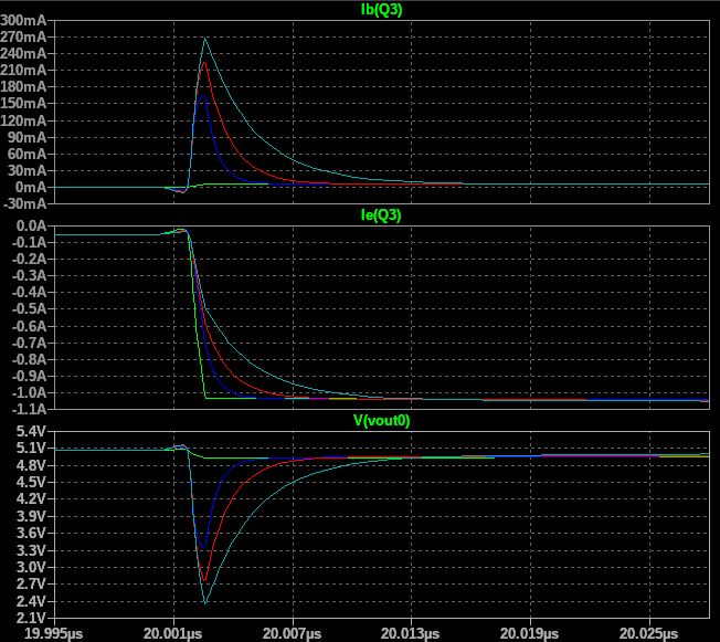
Variable base resistance with transit time set to 400ps
If base resistance is 0Ohm and transit time is not 0s, then, during the step load, betaF is maintained at its steady-state value and the NPN device keeps its linearity. When a non-zero base resistor is used,

Variable transit time with base resistance set to 0Ohm
Variable transit time with base resistance set to 10Ohm
Conclusion: pass device pole and the need for an output capacitor
As you can see from the simulation, we need an output capacitor because of the non-ideality of the pass device - we have to compensate for its delay in the output load step response: the output capacitor will provide most of the required load current until the pass device can restore a steady state condition in which the whole current comes from the pass device only. The main cause for this is the transit time (or lifetime across the BJT base) summed with the base resistor which introduces a pole in the system. Proper modelling requires a large signal model (charge control model) which is pretty complex so it will not be discussed here.
Share this page


Comments
Be polite and respectful in the comments section. In case of doubts, read this before posting.
Posted comments ⮧
Comment section still empty.
INDEX
2. BJT aspects involved in step load
3. Conclusion: pass device pole and the need for an output capacitor
INFO
STATISTICS
PREVIOUS ARTICLE
CONTACTS
SHARE