
Desaturation protection in high power systems
Desaturation protection is a mechanism designed to prevent damage to power devices, such as IGBTs or MOSFETs, during of short-circuit or overload. Let's analyse the physics of these events and the circuital implementation of this protection.
DESAT protection in high-voltage systems
All electronic power systems could experience failure due to bad design, misuse, overstress, infant mortality and many other reasons; however, in this article, I won't cover the analysis of all possible failure modes, nor the design tips one should adopt to avoid them; I will rather talk about one specific protection that modern applications always implement: desaturation protection.
The name is used equally for both bipolar and field-effect devices, even if the term 'desaturation' is related to the first ones: it means 'going out from saturation region', which is the desired operating region when using a bipolar device as a switch. DESAT protection is a circuit used to understand if, during conduction, the power device erroneously moves away from a fully on state.
Power devices as switches
To reduce power dissipation, switching with a defined duty cycle, then filtering the output with inductors and capacitors is better than building linear devices. For this purpose, a controller capable of acquiring some quantities, elaborating them and calculating a proper duty cycle to apply to the plant (a motor, a transformer, an inductor, a power line, ...) is needed. Such PWM command is sent to the driver, which has an output stage supplied with a higher voltage and proper current capability; the simple low-voltage command is turned into a higher voltage command that allows turning on and off the power device through its control terminal (base, gate, whatever).
What does it mean to turn on and off? Well, it means sending the power device in interdiction and conduction state, back and forth. However, since we want to have power dissipation as low as possible, we want to reduce the power lost by the device in those two states (let's ignore the switching losses, they are not relevant to this analysis).
Power dissipated while the transistor (diode, SCR, GTO ...) is off is $$P_{d,off} = V_{bus} I_{leak}$$ where Vbus is the supply voltage and Ileak is the leakage current flowing, for example, from drain to source in a MOSFET, even if it is kept safely off. This has a strong temperature dependence.
Power dissipated while the transistor (diode, SCR, GTO ...) is on is $$P_{d,on} = V_{ds,on} I_{load}$$ where Vt,on is the voltage appearing between, let's say, drain and source in a MOSFET while it's kept on and Iload is the current flowing from supply (or ground) to the load.
Let's do some analysis with a real power device! I've chosen the FAM65HR51DS1 component from ONSEMI. It contains four 650V-rated power MOSFETs in a H-bridge topology.
Static losses
When the device is off
When the device is off, power dissipation is negligible! If we use the devices at their maximum absolute voltage (that will never happen in real applications), the power loss is $$P_{d,off} = V_{bus} I_{leak} = 650V \cdot 10\mu A = 6.5mW$$ That's nothing compared to switching and conduction losses.

When the device is on
How much power is lost in the device while it's on? It's difficult to estimate it since it heavily depends on junction temperature, gate voltage level and load current. Let's take a look at some graphs from the selected device datasheet.
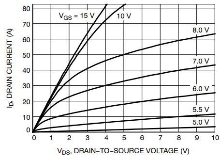
Here everything is fine: assuming our load sinks 50A with a duty cycle of 30% and we are driving the gate at 10V, the power dissipation would be $$P_{d,on} = duty V_{t,on} I_{load} = 0.3\cdot 50A \ cdot 2.5V = 37.5W$$ This H-bridge, operating under these conditions, should be dissipated for sure, since its junction temperature won't stay at 25°C when you run your system: it will warm up, leading static losses during on state to further increase! Let's see what happens if we don't cool down the device and the junction temperature reaches, for example, the extreme value of 150°C:

Well, if you don't design a good cooling system, this H-bridge device will surely blow up after a few seconds; at Tj=150°C the power loss becomes: $$P_{d,on} = duty V_{t,on} I_{load} = 0.3\cdot 50A \ cdot 55V = 825W \ !!!$$ Given the maximum load current, Vds may still vary with temperature, heavily affecting power dissipation! But how does all this Vds stuff relate to a protection mechanism?
Too-high-current failures
What happens if the output current is too high? What happens if two transistors short together, to the battery or ground? Well, a very high current pulse will flow through the MOSFET channel. This current is far beyond the maximum load current of your application (it can be thousands of Amperes) and could destroy the transistor. If you are working with high-voltage systems, physical damage of a power element could also generate a short circuit between high-voltage and low-voltage domains, posing a significant danger to people around. The best thing to do is to design proper protection circuits that, in case of too high current in the MOSFET, stop the actuation and forcibly turn off the MOSFET itself: this is what is called "Desaturation protection".
In case of currents outside specifications, MOSFET Vds will be pushed to a voltage higher than normal, which is far beyond the operating Vds (even at high ambient/air/cooling temperature): the best way to detect a very high current condition consists in acquiring the Vds as soon as the turn-on transition ends, and making sure that it's always under a chosen value; if it's over, then the circuit detects a DESAT event and will trigger a DESAT protection.
Note that, if the DESAT circuit is not properly tuned, you could detect a fault even if there is none! You have to ensure (by design) that your device Vds will never exceed a value of a few volts in normal operating conditions so that you'll be able to distinguish normal operation from a DESAT event! I wrote of power dissipation, temperature and Vds variability in previous paragraphs for this reason.
DESAT circuit
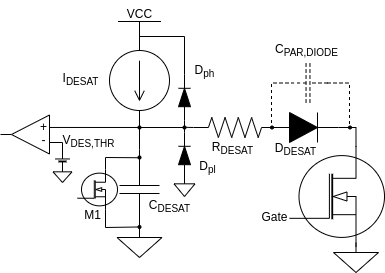
A simple desaturation circuit can be found here on the left.
Switch in OFF state
When the switch is off, it won't conduct any current so DESAT protection is not needed; the IDESAT current source is disabled and the output CDESAT is discharged through M1. The output of the DESAT comparator is ignored.
Switch in ON state
When the transistor is turned on, DESAT protection activates after a blanking time (usually a selectable value in the range of hundreds of ns to us). When the current source is enabled, a constant current flows in the output capacitor and, if Vds is low enough (power device fully conducting, no overcurrent or thermal overstress), the voltage across CDESAT won't rise over the selectable VDES,THR threshold, thanks to DDESAT that allows the current to flow in the power device.
On the contrary, if the power switch is conducting a too large current, its Vds will be so high that CDESAT will be charged up to the VDES,THR, triggering a DESAT fault detection.
Note that RDESAT can be used to fine-tune the threshold in case the comparator has too high values.
DESAT protection design
Now we have to choose the output capacitor, the resistor and the diode. Even if there are a few components, their choice must be operated with extreme care!
CDESAT
If too high, the circuit won't detect DESAT events fast enough to protect the power device. If too low, DESAT fault will be triggered because of noise and parasitic phenomena (see later). $$\Delta t = C_{DESAT} \frac{V_{des,thr}} {I_{DESAT}}$$ Knowing IDESAT, the designer can tune the capacitor and the programmable DESAT voltage to get the desired reaction time.
RDESAT and DDESAT
If R is too low, the DESAT circuit will trigger at too high currents. If R is too high, a false DESAT event could be detected. To ensure that DESAT protection won't trigger in normal operating conditions you have to satisfy $$V_{DES,THR} \gt V_{ds,opmax}\rvert_{T_j=T_{j,opmax}} + V_{f,DESAT-diode} + I_{DESAT}R_{DESAT}$$ $$V_{DES,THR} \lt V_{ds,ShortCircuitCurrent}\rvert_{T_j=T_{j,min}} + V_{f,DESAT-diode} + I_{DESAT}R_{DESAT}$$ We have to choose a diode that can sustain a reverse voltage equal to $$V_{r,DESAT-diode} \geq V_{bus,max} + L_{\sigma,SWITCH}\frac{di_{load}}{dt}$$ where Lσ,SWITCH is the stray inductance of the power transistor and the derivative represents the speed of the current transition at turn-off: this generates an extra voltage between the two terminals, drain and source in the case of a MOSFET.
Addendum
This circuit is simple and beautiful; it offers a great level of protection, ensuring power switch survival even in case of an abrupt short circuit. However, in high-voltage systems, where transients are really fast and energetic, parasitics become important!
CPAR,DIODE
This parasitic capacitance should be as low as possible: during turn-off, a large spike current may flow from the drain to the comparator pin through CPAR,DIODE, damaging the electronics! This is the reason why it is good to have RDESAT different from 0Ohm: it will provide aRC low pass filtering effect with CDESAT.
For this same reason, the DESAT circuit is typically made blind during turn-on and turn-off transitions, to make the system immune to fast transients that could be the source of false positive faults.
Share this page


Comments
Be polite and respectful in the comments section. In case of doubts, read this before posting.
Posted comments ⮧
Comment section still empty.
INDEX
INFO
STATISTICS
CONTACTS
SHARE