
Diode emulation mode
Diode emulation mode in switching converters for low-voltage, high-current applications
Buck converter in high-current applications
Buck converter is a simple and efficient step-down DC-DC converter, widely used in low-voltage, high-current applications. When power density rises and currents become very high, all the components are stressed much more. Some various strategies and countermeasures can be implemented: one of them is the so-called diode emulation mode.
It is supposed you already know how a buck converter works, so many descriptions and calculations are not shown in this article.
Losses in high-current bucks
When designing a buck converter for high-current applications, engineers typically have some desirable additional characteristics to meet: dissipating as little as possible, working at high frequency, using small-sized components and soon. However, they lead to other problems to account for during the development. Moreover, some of these requirements cannot be satisfied if a typical DCDC topology is used, so other solutions must be found.
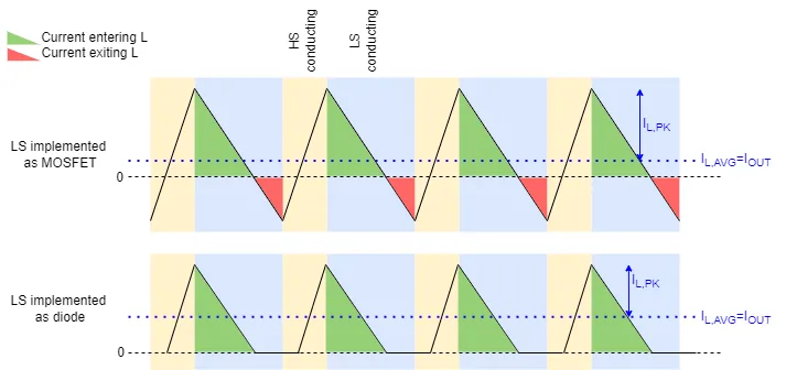
Let's start from the dissipation, which is the most relevant aspect when working on power electronics: old buck converters were designed with the low side switch implemented as a diode, to remove dead-time management and avoid thus shoot-through issues; however, such components have been replaced in most recent times by a MOSFET (synchronous buck) to remove the diode losses during forward polarization. In this case, the inductor current is always triangle-shaped and, if the load current is lower than half of the pk-to-pk inductor current (light load operating mode), the LS (low-side) MOSFET current will take both directions (drain to source and source to drain). Using MOSFETs as low-side switching components is a good solution to reduce conduction losses but inductors and capacitors are more stressed.
In the other case, if a diode is utilized as an LS switch, the power lost in the diode when it's in forward polarization is higher $$P_{fwd,diode} = V_{diode,avg} \cdot I_{diode,avg} > P_{cond,MOS} = R_{DS,on} \cdot I_{MOS,RMS}^2$$ However, in this configuration, the RMS inductor current is lower (the converter works in pure DCM) and the AC power loss reduces significantly; the same happens for capacitors, which see lower RMS currents. Moreover, when the inductor current goes to 0A, no reverse current is allowed to flow in the diode because of its blocking nature.
It is possible to see highly desirable behaviours in both topologies: synchronous bucks reduce conduction losses thanks to an LS element implemented as a MOSFET but more power is lost in the inductor and capacitors. On the other hand, classical bucks are less efficient but, when operating in DCM, RMS inductor and capacitor currents are lower. Diode emulation mode is an effective way to get benefits from both topologies!
Diode emulation
A MOSFET is used as an LS switch, and, under light load, it is turned off as soon as the inductor (and so LS MOSFET itself) current reaches 0A, like in a classical buck converter. In this way, LS conduction loss is lower (thanks to the MOSFET) and so for the inductor and capacitors, which must deal with lower RMS currents!
The converter under light load operates in DCM, the inductor can be kept small (conveniently increasing the switching frequency), LS switch conduction losses are proportional to Rds,on only, inductor AC losses and capacitors losses are lowered! This is one of the few cases in which a solution brings almost only positive aspects.
In light load operation, the LS MOSFET conduction losses are reduced since the current flowing through its channel is equal to the one passing through a diode in the case of a non-synchronous buck. $$P_{cond,MOS} = R_{DS,on} \cdot I_{diode,RMS}^2$$
Practical example
Let's design three bucks with the same input and output characteristics, exploiting the three different topologies; values are not necessarily realistic, they have been arranged to simplify calculations.
$$V_i = 5V$$ $$V_o = 1V$$ $$L = 1uH$$ $$f_{sw} = 100kHz$$ $$I_o = 1A$$ $$R_{L,DC} = R_{L,AC} = ESR = R_{DS,on} = 10mOhm$$ $$V_{fwd,diode} = 0.4V \quad (Schottky)$$ It's easy to calculate duty, pk-to-pk inductor currents and time intervals in the three cases.
Synchronous buck, light load
Here are the calculations for the synchronous buck $$D=\frac{V_o}{V_i}=20, \quad T_{on}=\frac{D}{f_{sw}}=2\mu s, \quad T_{off}=8\mu s$$ $$\Delta I_{L,pkpk}=\frac{V_i-V_o}{L}T_{on}=8A$$
Now, let's calculate the power dissipated on the various components $$P_{L,DC}=R_{L,DC}\cdot I_{L,RMS}^2 = 10mOhm\cdot (\frac{4^2}{3}+1^2)A^2 = 63mW$$ $$P_{L,AC}=R_{L,AC}\cdot I_{L,RMS}^2 = 10mOhm\cdot \frac{4^2}{3}A^2 = 53mW$$ $$P_{diss,Cout} = ESR\cdot I_{Cout,RMS}^2 = 10mOhm\cdot \frac{4^2}{3}A^2 = 53mW$$ $$P_{cond,MOS} = R_{DS,on}\cdot I_{LS,MOS}^2 = 10mOhm\cdot 13.1A^2 = 131mW$$
Classical buck, DCM
Here are the calculations for the classical buck $$D=10, \quad T_{on}=1\mu s, \quad T_{off}=4\mu s, \quad T_{idle}=5\mu s$$ $$\Delta I_{L,pkpk}=4A$$
Now, let's calculate the power dissipated on the various components $$P_{L,DC}=R_{L,DC}\cdot I_{L,RMS}^2 = 10mOhm\cdot \frac{10 \cdot 4^2}{3}A^2 = 53mW$$ $$P_{L,AC}=R_{L,AC}\cdot I_{L,RMS}^2 = 10mOhm\cdot \frac{10 \cdot 4^2}{3}A^2 = 53mW$$ $$P_{diss,Cout} = ESR\cdot I_{Cout,RMS}^2 = 10mOhm \cdot 1.96A^2 = 20mW$$ $$P_{fwd,diode} = V_{fwd,diode}\cdot I_{fwd,diode} = 0.8A \cdot 0.4V = 320mW$$
Synchronous buck with diode emulation
From the two previous sections, it is made clear that classical buck has high power dissipation on the diode during Toff. Diode emulation overcomes this problem, keeping more or less the same losses from the synch buck for the LS MOSFET and the same losses from the classical buck for the inductor and capacitors. $$P_{L,DC}=R_{L,DC}\cdot I_{L,RMS}^2 = 10mOhm\cdot \frac{10 \cdot 4^2}{3}A^2 = 53mW$$ $$P_{L,AC}=R_{L,AC}\cdot I_{L,RMS}^2 = 10mOhm\cdot \frac{10 \cdot 4^2}{3}A^2 = 53mW$$ $$P_{diss,Cout} = ESR\cdot I_{Cout,RMS}^2 = 10mOhm \cdot 1.96A^2 = 20mW$$ $$P_{cond,MOS} = R_{DS,on}\cdot I_{LS,MOS}^2 = 10mOhm\cdot 13.1A^2 = 131mW$$
Simulation
The previous three bucks have been simulated on LTspice (only SS, open loop).

In diode emulation mode, peak currents are the lowest in both MOSFETs and inductor; the capacitor supplies a reduced RMS current; moreover, duty is lower with respect to classical buck as in this configuration there is no need to recover from the additional forward voltage drop of the LS diode.

Drawbacks
Complexity
The buck controller gains in complexity: it needs a circuit that turns off the LS MOSFET when the zero crossing point of the inductor current is sensed (for the sake of simplicity, this sensing can be implemented through a low-side resistor on the MOSFET source).
Negative transient
Particular attention must be paid during turn-on transient: before the buck is enabled, some residual charges may keep the voltage on the output capacitor high. When the low-side MOSFET is enabled, a steep negative transient voltage could appear at the output supply rail, damaging the load. To prevent this, an output discharge circuit should be considered.

Share this page


Comments
Be polite and respectful in the comments section. In case of doubts, read this before posting.
Posted comments ⮧
Comment section still empty.
INDEX
INFO
STATISTICS
CONTACTS
SHARE