➔ Index of ⦁ Bridge Topology - Models and Calculations ⦁
Bridges - Part III: Full-Bridge
Detailed analysis of the full-bridge topology, with schemes and calculations
Full bridge
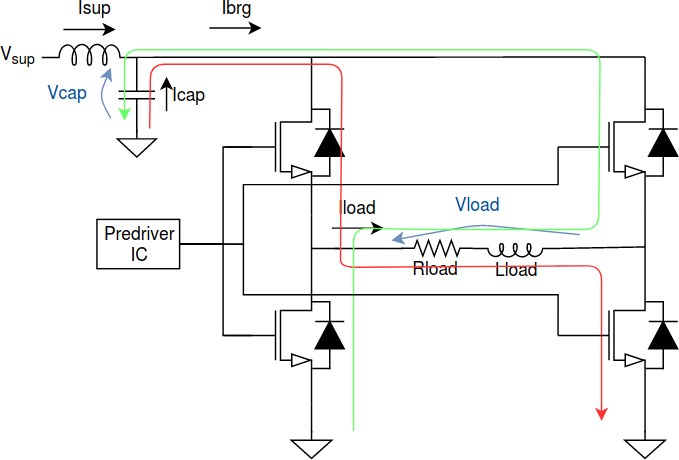
The full bridge simplified circuit to be taken as reference is shown below. The push-pull version is analyzed here: it is composed by four switches (two low side and two high side ones) and an input LC filter.
The full bridge equations are listed below. You will see that with full bridge input capacitor RMS current increases, ripple current is doubled, power losses increases, so, why using full bridge? Easy: in the full bridge topology the load current can be driven in both directions, so, use it only if strictly necessary.
Load analysis
The ideal voltage seen by the load is a square wave $$V_{load}(t) = 2V_{sup} \cdot squarewave(T,D)(t)- V_{sup}$$
The average voltage and current in the load are shown below $$V_{load,avg} = \frac{V_{sup} T_{on}-V_{sup} T_{off}}{T} = V_{sup} (2D-1)$$ $$I_{load,avg} = \frac{V_{load,avg}}{R_{load}}$$ $$V_{Lload}(t) = 2V_{sup} \cdot squarewave(T,D)(t) - V_{sup} - V_{load,avg}$$ $$V_{Rload}(t) = V_{load}(t) - V_{Lload}(t) = V_{load,avg}$$
Since we are working with an inductive load, the integral of the voltage over the time in the inductive part of the load must be zero. $$\int_{0}^{T} V_{Lload}(t) dt = 0$$
The voltage seen by the load inductor is the supply voltage minus the average voltage over the time. The current ripple is described by the common inductor law $$V_{Lload@Ton} = V_{sup}-V_{load,avg} \quad , \quad V_{Lload@Toff} = -V_{sup}-V_{load,avg}$$ $$\Delta I_{load,pkpk} = \frac{V_{Lload@Ton}}{L} T_{on} = \frac{V_{sup}-V_{load,avg}}{L} D T = \frac{2V_{sup}}{L f} (1-D) D$$
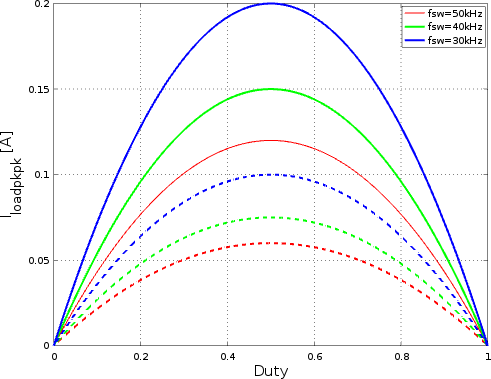
Since the pkpk inductor current depends on the duty, its maximum is reached when the duty cycle is set to 50%. In the following image the supply voltage was set to 12V and the load inductance to 1mH. The ripple current obtained with the full bridge is double with respect to the half bridge configuration, with same L, switching frequency and battery voltage.
Input Capacitor analysis
Current analysis
In order to find the most appropriate input capacitor, some calculations must be done. Input capacitor is part of an LC undamped filter which decouples the average current to be provided by the supply and the AC current required by the load: all the following formulas are valid under the assumption that the input filter inductor provides only the DC component of the overall bridge current and the filter capacitor only the AC component; in the real world, a small AC current comes from the supply too but in this case such contribution is neglected. All the following calculations are done under the assumption that (signs are coherent with the reference image): $$I_{brg}(t)=I_{sup}(t)+I_{cap}(t)$$ All the following calculations are unrelated to the capacitor size but they are dependent on the system only!
The equations of the bridge current are the following ones (in the full bridge configuration, the bridge current is different from 0 both at D and at D' instants): $$I_{brg,low@Ton} = I_{load,avg} - \frac{\Delta I_{load,pkpk}}{2}$$ $$I_{brg,high@Ton} = I_{load,avg} + \frac{\Delta I_{load,pkpk}}{2}$$ $$I_{brg,low@Toff} = -I_{load,avg} - \frac{\Delta I_{load,pkpk}}{2}$$ $$I_{brg,high@Toff} = -I_{load,avg} + \frac{\Delta I_{load,pkpk}}{2}$$ $$I_{sup} = I_{brg,avg} = \frac{I_{load,avg} T_{on}}{T} - \frac{I_{load,avg} T_{off}}{T} = I_{load,avg}(2D-1)$$
It is now possible to calculate the current in the input capacitor. During the turn on phase (high side switch on, low side off), the load current is provided by the input capacitor and the supply and during turn off the load current goes in the input capacitor: in the full bridge configuration the input capacitor is stressed more since it is used both during turn on and turn off phases. $$I_{cap,low@Ton} = I_{brg,low@Ton} - I_{sup} \quad , \quad I_{cap,high@Ton} = I_{brg,high@Ton} - I_{sup}$$ $$Q_{cap@Ton} = \frac{(I_{cap,low@Ton} + I_{cap,high@Ton}) T_{on}}{2} = \frac{2I_{load,avg} D (1-D)}{f}$$
During the turn off phase (high side switch off, low side on), the load current recirculates in the low side switch (channel or body diode, depending on the current value) and the capacitor is charged at a constant current. $$I_{cap,low@Toff} = I_{brg,low@Toff} - I_{sup} \quad , \quad I_{cap,high@Toff} = I_{brg,high@Toff} - I_{sup}$$ $$Q_{cap@Toff} = \frac{(I_{cap,low@Toff} + I_{cap,high@Toff}) T_{off}}{2} = \frac{-2I_{load,avg} D (1-D)}{f}$$
As you can see the charge balance in the capacitor is ensured. $$Q_{cap@Toff} = -Q_{cap@Ton}$$
The overall RMS current in the capacitor can be calculated with the well known formula: $$I_{cap,RMS} = \sqrt{\frac{1}{T} \int_{0}^{T} I_{cap}^2(t) dt} = \sqrt{\frac{1}{T} \Bigl(\int_{0}^{T_{on}} I_{cap@Ton}^2(t) dt + \int_{Ton}^{T} I_{cap@Toff}^2(t) dt\Bigr)}$$ Now we can divide the RMS current calculation in two parts: one related to Ton (RMS of a trapezoid wave) and the second one to Toff (RMS of a trapezoidal wave). $$I_{cap,RMS@Ton} = \sqrt{\frac{D}{3} \Bigl(I_{cap,low@Ton}^2 + I_{cap,high@Ton}^2 + I_{cap,low@Ton} I_{cap,high@Ton}\Bigr)}$$ $$I_{cap,RMS@Toff} = \sqrt{\frac{D}{3} \Bigl(I_{cap,low@Toff}^2 + I_{cap,high@Toff}^2 + I_{cap,low@Toff} I_{cap,high@Toff}\Bigr)}$$ $$I_{cap,RMS} = \sqrt{I_{cap,RMS@Ton}^2 + I_{cap,RMS@Toff}^2}$$ So, after all these calculations, the chosen capacitor must be able to provide the required RMS current (possibly with some margin). Remeber that all bulk capacitor are usually electrolytic ones and they all have a derating factor to be applied to the maximum RMS current when switching frequency is lower than - typically - 100kHz.
Voltage analysis
Once the maximum input capacitor ripple current has been found, the capacitor size must be calculated; the following formula is enough. $$\Delta V_{cap,pkpk}=\frac{\Delta Q_{cap@Ton}}{C}=\frac{2I_{load,avg} D (1-D)}{f C}$$ Note that, again, the maximum ripple voltage on the input capacitor is obtained when D=50% and it is doubled with respect to the half bridge configuration.
Power losses
Input inductor power loss
Input inductor filter power loss depends on the series resistance of the inductor itself and the average current drained from the power source. $$P_{loss,L}=I_{brg,avg}^2DCR_{ind}$$
Input capacitor power loss
Input capacitor power loss is due to the ESR of the capacitor itself which is ideally the only parasitic contribution. Noth that the ESR of a capacitor changes with the frequency so the right value has to be used in this formula. $$P_{loss,cap}=I_{cap,RMS}^2ESR_{cap@f}$$
Model
Share this page


Comments
Be polite and respectful in the comments section. In case of doubts, read this before posting.
Posted comments ⮧
Comment section still empty.
INDEX
INFO
STATISTICS
PREVIOUS ARTICLE
NEXT ARTICLE
CONTACTS
SHARE