
Active Miller Clamp
What is Active Miller Clamp? In modern high-voltage systems, protection circuits are mandatory to ensure a high safety level of the product. Let's analyse this well-known feature and its hardware implementation.
Power transistors parasitics
In power electronics, half-bridge topology is used in many fields but some troublesome phenomena are visible only when working in high voltage/high current applications. One of the worst problems that can occur in a bad design is cross conduction, the event that sees both high and low-side transistors conducting at the same time, even for a short time.
If this happens, failure and permanent physical damage can occur, so the designer must avoid this condition. Dead time is the first solution and it allows the high side to switch on only when the low side is safely off and vice versa; however, sometimes, this is not enough: under some operating conditions and in specific applications, it may happen that the non-conducting transistor switches on unwantedly because of some parasitics element! Moreover, there is no way to detect such behaviour during the application lifetime! This effect is called parasitic turn-on and it is typical of high-voltage systems working with fast transistors.
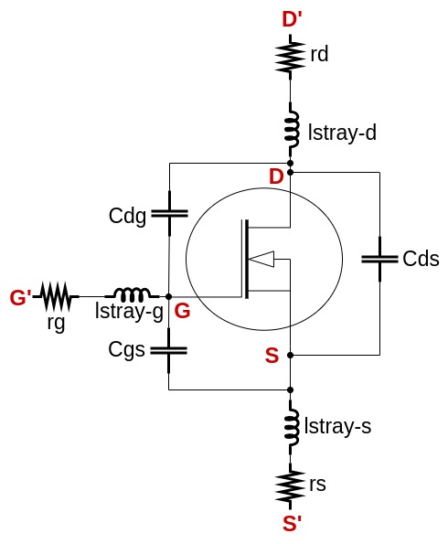
In the image on the right you can see the parasitics elements of a MOSFET.
- rd This series resistance models the resistance between the solder joint or the tab and the die at the drain terminal. rd causes power losses during the conduction
- rg This series resistance models the resistance between the solder joint or the tab and the die at the gate terminal. rg causes power losses during commutation and prevents the driver from having full control over the gate voltage
- rs This series resistance models the resistance between the solder joint or the tab and the die at the source terminal. rs causes power losses during the conduction
- lstray-d This series inductance models the parasitic inductor between the solder joint or the tab and the die at the source terminal. lstray-d causes voltage overshoot during commutation (at turn-off)
- lstray-g This series inductance models the parasitic inductor between the solder joint or the tab and the die at the gate terminal. lstray-g causes voltage overshoot and uncontrolled ringing at the gate terminal during commutation and slows down gate voltage transition
- lstray-s This series inductance models the parasitic inductor between the solder joint or the tab and the die at the source terminal. lstray-s causes voltage overshoot during commutation (at turn-off)
- Cds This parallel capacitor models the parasitic capacitor in the transistor vertical structure present at the p-n interface. It generates very fast current spikes in the channel at turn-on
- Cgs This capacitor models the gate capacitance and must be charged and discharged to allow the transistor to switch on and off. During transient it can be partially charged or discharged by parasitic phenomena.
- Cdg This is sometimes called Miller capacitance and it is a parasitic component whose effect is disruptive during commutation since charge injection can happen through such capacitor towards Cgs
All the stray elements listed above are involved in the parasitic turn-on but the most important one is the Cdg: the higher, the worse!
Unwanted effect during commutation: parasitic turn-on
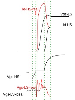
waveform in a MOSFET
During commutation, very fast voltage and current transients happen in the switching transistor. These abrupt and fast events can affect also other components in the circuit so we have to find a workaround to make it work smoothly.
Here on the left, you can see an example of voltage/current commutation of an H-bridge (HS and LS MOSFET) in a high voltage and high current application, over an inductive load. As you can see, when the HS MOSFET turns on, a parasitic current may flow inside the gate of the LS transistor through Cdg, causing the LS MOSFET gate voltage to increase and, eventually, to exceed the threshold voltage. If this happens, both HS and LS will be conducting at the same time, dramatically increasing the switching power losses and, eventually, leading the power transistors to permanent damage.
AMC is the solution
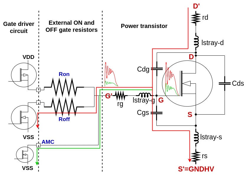
To remove this problem, AMC is typically implemented, both as discrete circuitry or directly inside the gate driver. It consists of a low-side transistor which is switched on as soon as the turn-off transition is completed: in this way the gate is directly clamped to the VSS of the power supply in the HV domain, bypassing the gate resistors. The charge injected, for example, from the HS MOSFET channel into the LS MOSFET gate (passing through the LS MOSFET Cdg capacitance) is almost completely absorbed by the AMC MOSFET and so no unwanted voltage arises at the G terminal.
Actually, because of rg and lstray-g, a residual phenomenon still happens inside the package of the transistor at the G terminal, since the designer can operate only at the G' terminal (which is the one externally available). To be sure that no parasitic turn-on happens in any case, it is good practice to turn off the transistor with a negative voltage and to have the AMC MOSFET source connected to VSS rather than S'=GNDHV. VSS is a negative voltage with respect to GNDHV, which, instead, is the 0V in the high voltage domain for the power transistor.
Share this page


Comments
Be polite and respectful in the comments section. In case of doubts, read this before posting.
Posted comments ⮧
Comment section still empty.
INDEX
INFO
STATISTICS
CONTACTS
SHARE