➔ Index of ⦁ Boost converter ⦁
Boost converter - Voltage mode AC model
AC small signal model for a generic boost regulator controlled in voltage mode (VMC)
Voltage mode control
Boost converter can be controlled in voltage mode (VMC), which means that only the output voltage is used as feedback to the controller. This control mode simple; however, the boost controller has a bad feature: the Gvd transfer function has a double resonant pole and a right half-plane zero! We have to design a proper compensation network to boost the phase around the crossover frequency.
AC small signal model
Starting from DC model
To find the AC model, we can start with the DC model of the converter $$\begin{cases} v_L = D(v_I)+D'(v_I-v_O) = L\frac{di_L}{dt} \\ i_C = D(-\frac{v_O}{R})+D'(i_L-\frac{v_O}{R}) = C\frac{dv_O}{dt} \end{cases}$$ Let's simplify $$\begin{cases} v_L = v_I-v_O+Dv_O = L\frac{di_L}{dt} \\ i_C = i_L(1-D)-\frac{v_O}{R} = C\frac{dv_O}{dt} \end{cases}$$ Let's add also the equation related to the input current $$i_I = i_L = \frac{1}{D'}i_O$$
Perturb and Linearize
Now we can add a small perturbation to all the terms in the previous system $$\begin{cases} (V_I+\hat v_I)-(V_O+\hat v_O)+(D+\hat d)(V_O+\hat v_O) = L\frac{d}{dt}(I_L+\hat i_L) \\ (I_L+\hat i_L)-(D+\hat d)(I_L+\hat i_L)-(\frac{V_O+\hat v_O}{R}) = C\frac{d}{dt}(V_O+\hat v_O) \end{cases}$$ Let's group DC (constant), SS (first order, small signal) and non-linear terms $$\begin{cases} V_I - V_O + DV_O + \hat v_I - \hat v_O + D \hat v_O + \hat d V_O + \hat d \hat v_O= L\frac{d}{dt}(I_L+\hat i_L) \\ I_L - DI_L - \frac{V_O}{R} + \hat i_L - D\hat i_L - I_L \hat d - \frac{\hat v_O}{R} - \hat d \hat i_L = C\frac{d}{dt}(V_O+\hat v_O) \end{cases}$$ Let's do the same for the input equation $$I_I + \hat i_i = \frac{I_O + \hat i_o}{D'+ \hat d'}$$ and now, let's group terms by order $$I_I + \hat i_i = \frac{I_O}{D'} + \frac{I_O}{\hat d'} + \frac{\hat i_o}{D'} + \frac{\hat i_o}{\hat d'} $$
Simplifications
Since we want to find a linear model, we can remove unnecessary terms (DC and second or eventually higher order terms) $$\begin{cases} \hat v_I - \hat v_O + D \hat v_O + \hat d V_O = L\frac{d}{dt}(\hat i_L) \\ \hat i_L - D\hat i_L - I_L \hat d - \frac{\hat v_O}{R} = C\frac{d}{dt}(\hat v_O) \end{cases}$$ The input equation becomes $$\hat i_i = \frac{I_O}{\hat d'} + \frac{\hat i_o}{D'}$$
Laplace transform
Now we can go into the frequency domain and substitute the second equation in the first one $$\begin{cases} \hat i_L (1-D)= sC\hat v_O + \frac{\hat v_O}{R} + \hat d I_L \\ \hat v_I - \hat v_O + D\hat v_O + \hat d V_O = sL \hat i_L \end{cases}$$ Rearranging terms we get $$\begin{cases} \hat i_L = \frac{sC\hat v_O + \frac{\hat v_O}{R} + \hat d I_L}{1-D} \\ \hat v_O = \hat d \frac{V_O}{D'}\frac{1-\frac{sLI_L}{D'V_O}}{s^2 \frac{LC}{D'^2} + s \frac{L}{RD'^2} + 1} + \hat v_I \frac{1}{D'}\frac{1}{s^2 \frac{LC}{D'^2} + s \frac{L}{RD'^2} + 1} \end{cases}$$ and finally $$\begin{cases} \hat i_L = \frac{\hat v_O(sC + \frac{1}{R}) + \hat d I_L}{1-D} \\ \hat v_O = \hat d \frac{V_O}{D'}\frac{1-\frac{sLI_L}{D'V_O}}{s^2 \frac{LC}{D'^2} + s \frac{L}{RD'^2} + 1} + \hat v_I \frac{1}{D'}\frac{1}{s^2 \frac{LC}{D'^2} + s \frac{L}{RD'^2} + 1} \end{cases}$$ Remembering that Vo=Vi/D' and IL=II=Io/D', the equations become $$\begin{cases} \hat i_L = \frac{\hat v_O(sC + \frac{1}{R}) + \hat d I_L}{1-D} \\ \hat v_O = \hat d \frac{V_O}{D'}\frac{1-\frac{sL}{D'^2 R}}{s^2 \frac{LC}{D'^2} + s \frac{L}{RD'^2} + 1} + \hat v_I \frac{1}{D'}\frac{1}{s^2 \frac{LC}{D'^2} + s \frac{L}{RD'^2} + 1} \end{cases}$$ Now, I want to find the relation between the inductor current with respect to duty cycle and input voltage variations. Let's substitute the second equation in the first one. $$\begin{cases} \hat i_L = \hat d \frac{2V_O}{RD'^2} \frac{(s\frac{CR}{2} + 1)}{s^2 \frac{LC}{D'^2} + s \frac{L}{RD'^2} + 1} + \hat v_I \frac{1}{D'^2}\frac{sC + \frac{1}{R}}{s^2 \frac{LC}{D'^2} + s \frac{L}{RD'^2} + 1}\\ \hat v_O = \hat d \frac{V_O}{D'}\frac{1-\frac{sL}{D'^2 R}}{s^2 \frac{LC}{D'^2} + s \frac{L}{RD'^2} + 1} + \hat v_I \frac{1}{D'}\frac{1}{s^2 \frac{LC}{D'^2} + s \frac{L}{RD'^2} + 1} \end{cases}$$ The input equation in the frequency domain remains unchanged $$\hat i_i = \frac{I_O}{\hat d'} + \frac{\hat i_o}{D'}$$
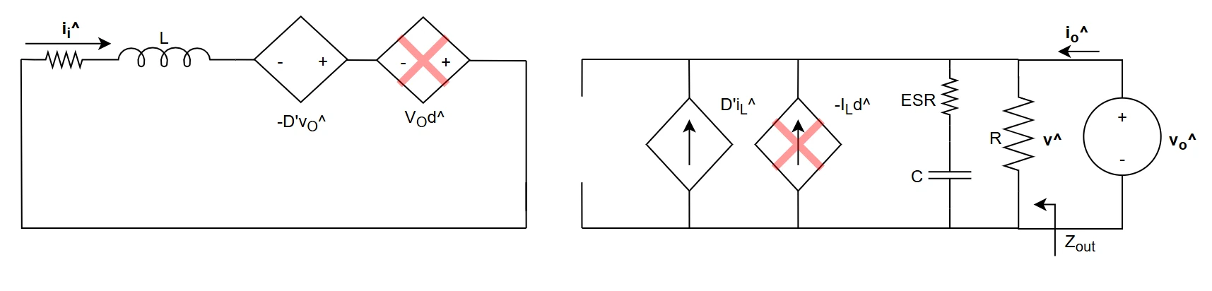
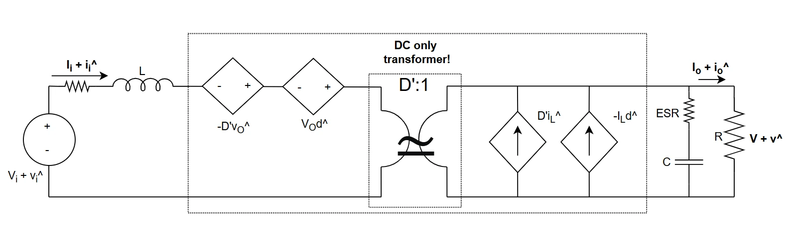
Scheme of the model
Let's draw the scheme of the model, considering all the DC and first order terms and neglecting the higher order ones.
Control to Output transfer function
In the previous paragraph I have found the Gvd transfer function, which is the Duty-to-Output relation, the power stage transfer function. However, since the duty cycle is generated with a well-defined modulation scheme, it is good practice to go on to find the Control-to-Output tf, which is the relationship between a control voltage and the output voltage. Control voltage strictly depends on the circuital implementation of the modulator. For boost converters in voltage mode, the modulator is just a set-reset flip flop connected to a circuit which compares the control voltage (output of the error amplifier) with a triangle wave (ramp): it is easy to see that the control voltage over the ramp gives the duty cycle. $$V_C(t) = D(t) V_{ramp,pk} \rightarrow V_C + \hat v_c = (D + \hat d) V_{ramp,pk} \rightarrow \hat v_c = \hat d V_{ramp,pk}$$
The final Control-to-Output function is $$\frac{\hat v_O}{\hat v_c} = \frac{1}{V_{ramp,pk}} \frac{V_O}{D'}\frac{1-\frac{sL}{D'^2 R}}{s^2 \frac{LC}{D'^2} + s \frac{L}{RD'^2} + 1}$$
Power stage transfer functions
List of ideal open loop transfer functions; parasitic elements like ESR, DCR, Rdson, Vd are not considered. $$\begin{align} &G_{vd} = \frac{\hat v_O}{\hat d} = \frac{V_O}{D'}\frac{1-\frac{sL}{D'^2 R}}{s^2 \frac{LC}{D'^2} + s \frac{L}{RD'^2} + 1} \quad Duty-to-Output\\ &G_{vv} = \frac{\hat v_O}{\hat v_I} = \frac{1}{D'}\frac{1}{s^2 \frac{LC}{D'^2} + s \frac{L}{RD'^2} + 1} \quad Input-to-Output\\ &G_{id} = \frac{\hat i_L}{\hat d} = \frac{2V_O}{RD'^2} \frac{(s\frac{CR}{2} + 1)}{s^2 \frac{LC}{D'^2} + s \frac{L}{RD'^2} + 1} \quad Duty-to-InductorCurrent\\ &G_{iv} = \frac{\hat i_L}{\hat v_I} = \frac{1}{D'^2}\frac{sC + \frac{1}{R}}{s^2 \frac{LC}{D'^2} + s \frac{L}{RD'^2} + 1} \quad Input-to-InductorCurrent \end{align}$$ Control-to-Output transfer function with a very simple triangle wave modulator. $$G_{vc} = \frac{\hat v_O}{\hat v_C} = \frac{1}{V_{ramp,pk}} \frac{V_O}{D'}\frac{1-\frac{sL}{D'^2 R}}{s^2 \frac{LC}{D'^2} + s \frac{L}{RD'^2} + 1} \quad Control-to-Output$$
Share this page


Comments
Be polite and respectful in the comments section. In case of doubts, read this before posting.
Posted comments ⮧
Comment section still empty.
INDEX
INFO
STATISTICS
PREVIOUS ARTICLE
NEXT ARTICLE
CONTACTS
SHARE