➔ Index of ⦁ Introduction to Digital Electronics ⦁
Digital electronics - Sequential logic
A quick look to sequential logic and basic devices
Sequential logic
With the expression 'sequential logic', we point at all those timed circuits, whose output depends not only on the current input but also on the previous ones. Sequential logic is typically implemented using devices that provide outputs according to stable inputs and a timing signal called 'clock'. The clock is usually a 50% duty cycle square wave, spread among the various subunits communicating with each other, necessary to synchronize their operations and their data exchange; for this reason, such systems are called 'synchronous'. As you can imagine, all the intermediate operations, made by combinational logic blocks, must be completed between a clock period and the next one.
Synchronous vs Asynchronous
Optimization of sequential logic
As for combinational logic, sequential logic can be simplified too, but in this case, methods can be very heterogeneous and complex, according to the type of device we are designing.
- Architectural level This must be done during the earliest stages since a change in the architecture can invalidate the whole design! When we talk of architectural optimization we talk about the definition of the pipeline, the number of combinational subunits in the datapath, the scheduling algorithm, the definition of parallelism and so on. As you can see, the designer can operate in many ways
- Implementation level You can optimize the design changing some choices during the description of the hardware, optimizing the subunit, changing the scheduling strategy in a refined way, adding another fetch stage to increase the level of parallelism
- Physical level As for the combinational logic, also for sequential one we can choose a different technology that could offer better performances
- Other techniques Clock or power gating, register disabling, clock frequency reduction, and dual Vth are examples of other techniques that can be used to reduce the power dissipation of the device. They are extensively used, especially in microcontroller design
These methods will be described in the next articles since they deserve particular attention.
Flip flops
As I did for the combinational logic article, I will provide an example of a sequential logic basic device: the very famous flop-flop. Flip-flops are used everywhere in modern digital sequential circuits; they are the core device behind registers, caches, and RAMs. It is a simple memory element, whose output is kept constant until a clock event happens. According to the type of flip-flop, we can have slightly different behaviours. In the schematics, flip-flops typically have a Q output (the main one), a Q' output (the negated output) and a small triangle which represents the clock input.
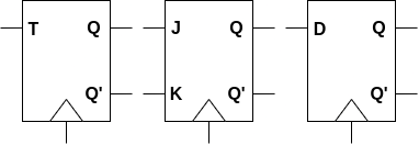
T flop-flop
T stands for 'toggle'; this flip-flop type can flip the output value Q if T is high and retain the old data if T is low. T flip-flop can be used as a frequency divider, since the output Q will run at half of the clock frequency as long as the T input is held high. If T is held low, instead, it will retain the data value indefinitely. $$\begin{array} {} T & Q & Q_{next} & Operation \\ 0 & 0 & 0 & Hold \\ 0 & 1 & 1 & Hold \\ 1 & 0 & 1 & Toggle \\ 1 & 1 & 0 & Toggle \end{array}$$
JK flop-flop
JK flip-flops are an extension of SR latches and can do many things all-in-one, just by setting the right values at its inputs: in fact, it can toggle the output, set it, reset it and keep the previously stored value. A very versatile device! $$\begin{array} {} J & K & Q & Q_{next} & Operation\\ 0 & 0 & 0 & 0 & Hold \\ 0 & 0 & 1 & 1 & Hold \\ 0 & 1 & 0 & 0 & Reset \\ 0 & 1 & 1 & 0 & Reset\\ 1 & 0 & 0 & 1 & Set \\ 1 & 0 & 1 & 1 & Set \\ 1 & 1 & 0 & 1 & Toggle \\ 1 & 1 & 1 & 0 & Toggle \end{array}$$
D flop-flop
This is probably the most used sequential device in the world. It can keep the stored data during the clock cycle and update its output in the next one. $$\begin{array} {} D & Q & Q_{next} & Operation \\ 0 & 0 & 0 & Update \\ 0 & 1 & 0 & Update \\ 1 & 0 & 1 & Update \\ 1 & 1 & 1 & Update \end{array}$$
The concept of clock
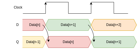
In the previous paragraphs I talked of the clock signal, saying that it is a synchronisation signal, running at a very precise frequency, used to make the whole combinational and sequential logic to perform operations in an ordered way. Now, let's understand better how a digital system works and why the clock is so important.

numbers and than a third value to the previous sum.
In the image on the side you can see that the combinational logic is typically enclosed between sequential logic blocks, which are employed to provide some 'periodicity' to the operation. This is exactly how modern digital circuits are made, regardless if the chip is a scalar, vectorial processor, an ASIC or an FPGA-based circuit. So, taking the image as a reference, when the clock signal has a rising edge the first two D flip-flops update their output value with the value at their input. During that clock period, the first 4-bit adder generated the sum which arrives at the input of the second flip-flop 'barrier' with some delay, but before the next clock rising edge. When this clock event happens, the result of the first sum is passed to the output of the second flop-flop 'barrier' and is processed by the second adder. The output will be updated with the right value at the third clock rising edge. As you can see, the clock is the master signal that makes the whole machine advance in its operations: at every clock cycle one more step is done toward the output.
In the image below you can see graphically how a sequential circuit updates the output of each stage at the next clock rising edge. During the time between one rising edge and another, all the combinational logic calculates the outputs to be sent to the next stage at the next clock rising edge.
Conclusions
In the next articles we will talk about the main properties of combinational and sequential logic and how they affect circuital design.
Share this page


Comments
Be polite and respectful in the comments section. In case of doubts, read this before posting.
Posted comments ⮧
Comment section still empty.
INDEX
INFO
STATISTICS
PREVIOUS ARTICLE
NEXT ARTICLE
CONTACTS
SHARE