➔ Index of ⦁ Introduction to Digital Electronics ⦁
Digital electronics - Combinational logic
What is meant with the expression 'combinational logic' and which are its main characteristics to account for during digital design
Combinational logic
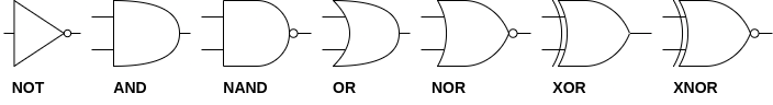
Combinational logic is the term used to point at all those circuits that, when stimulated with proper input, produce an output in no time, ideally without delay. They can be written on paper through algebraic expressions that completely describe their behaviour in terms of elementary binary operations. The simplest combinational logic gate is the NOT gate: it generates at the output a signal whose value is logically opposite to the input value. On the other hand, complex combinational circuits can be represented by those in ASICs, CPU and microcontroller datapaths, programmed FPGAs and CPLDs. Some of those circuits will be described in the next articles.
Improvement methods for combinational circuits
When a combinational circuit is very simple it cannot be simplified or made faster. However, when the functionality of the circuit becomes more and more complex, many methods can be operated to simplify the circuit. Eventually, come of these techniques help to reduce area and power dissipation, and to increase its speed and efficiency. Combinational circuits can be improved at various levels, as listed below:
- Architectural level The designer can improve the combinational logic by changing the circuit and the algorithm to implement the desired functions. For example, there are many types of a digital binary adder, so you can choose the fastest one instead of always using the simple but slow Ripple Carry Adder
- RTL level When the number of gates increases a lot (modern combinational logic can be made of thousands and thousands of gates), simplification is mandatory: it consists mainly of gate reduction that can be operated manually - by finding paths that are never taken or gates that are never excited - or automatically, through specific algorithms that take a circuital HDL description as input and return a simplified version of the same circuit, doing the same operation with a lower number of gates
- Physical level If your design already implements the best and most optimized algorithms to perform a binary operation and it is already exploiting the best techniques for gate reduction but it is still too slow, big or inefficient, the only thing you can further improve is its physical realisation: with exactly the same algorithm and HDL description, you can change the technology and get better performance
The same 3-step approach can be used not only for combinational logic but also for sequential logic and for the whole chip you design.
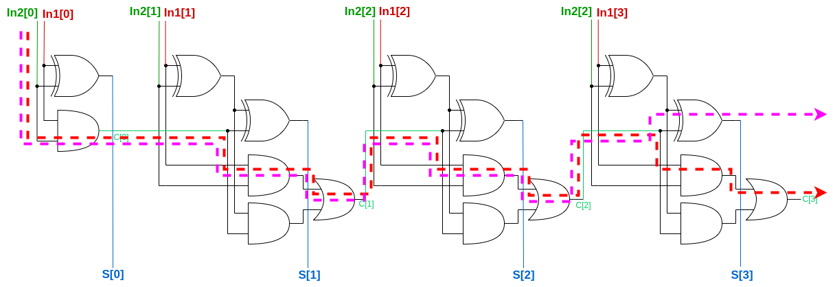
Ripple Carry Adder
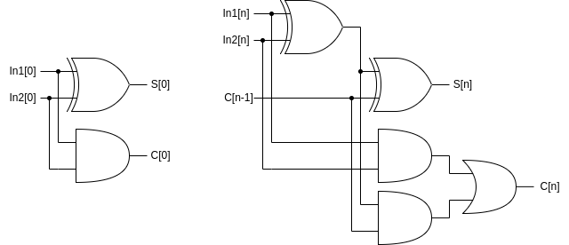
RCA is the simplest adder you can design to add two binary operands. It is made of a repetition of the elementary cell shown on the right in the image (called 'Full Adder'), up to the number of bits of the two operands. The cell on the left (called instead 'Half Adder') can be used to generate the sum and the carry bits of the two addends LSBs.
Algebraic expression
The algebraic expressions of the RCA elementary cell (full adder only), for both the sum and the carry bits are $$S[n] = In1[n] \oplus In2[n] \oplus C[n-1]$$ $$C[n] = (In1[n] \cdot In2[n]) + ((In1[n] \oplus In2[n]) \cdot C[n-1])$$
Time analysis
The output of the elementary cell is provided ideally in no time, as soon as the input changes. This is, obviously, not realistic, so we can evaluate the propagation delay input-to-output of the Full Adder, which is equal to the highest propagation delay between the sum generation path and the carry generation path. $$t_{pd,S[n]} = t_{pd,XOR} + t_{pd,XOR} = 2t_{pd,XOR}$$ $$t_{pd,C[n]} = t_{pd,XOR} + t_{pd,AND} + t_{pd,OR}$$ $$t_{pd,FA} = max(t_{pd,S[n]},t_{pd,C[n]})$$ The propagation delay of the Half Adder is instead $$t_{pd,HA} = max(t_{pd,XOR},t_{pd,AND})$$ Said n the number of bits of the two operands, the overall propagation delay of the Ripple Carry Adder is $$t_{pd,RCA} = t_{pd,HA} + (n-1)t_{pd,FA}$$
Conclusions
In this article one can find a very simple approach to digital electronics, especially combinational logic design, with a basic example. In the next article, you'll find an introduction to sequential logic, what it is and how it works.
Share this page


Comments
Be polite and respectful in the comments section. In case of doubts, read this before posting.
Posted comments ⮧
Comment section still empty.
INDEX
INFO
STATISTICS
PREVIOUS ARTICLE
NEXT ARTICLE
CONTACTS
SHARE