➔ Index of ⦁ Introduction to Digital Electronics ⦁
Digital design - Timing non-idealities
Which are the main timing-related quantities that should be considered when implementing a digital circuit? How do they affect your design?
Timing non-idealities
In previous articles, we treated digital signals as waves with perfectly sharp edges and no distortion, and digital circuits as a series of digital gates and memory elements as paths with no delay. This is not realistic and the ideal approximation can be made when the digital circuit works at low frequencies, with interconnections among the various subunits as short as possible. In all the other cases, it is crucial to understand the non-idealities of digital signals and all those delays that can affect the system operation. Forgetting some of them, even along one of the many paths, could invalidate the design entirely! Fortunately, EDA tools (computer-aided software designed to help the designer develop digital systems, test their proper functionality and analyse their performance) always have integrated timing analysis functions; this topic will be covered in the next article.
Timing non-idealities originate from interconnection parasitic elements, mainly series resistance along wires and wires capacitance, gate delay, gate output drive strength, and intrinsic properties of logic gates and memories.
Propagation delay

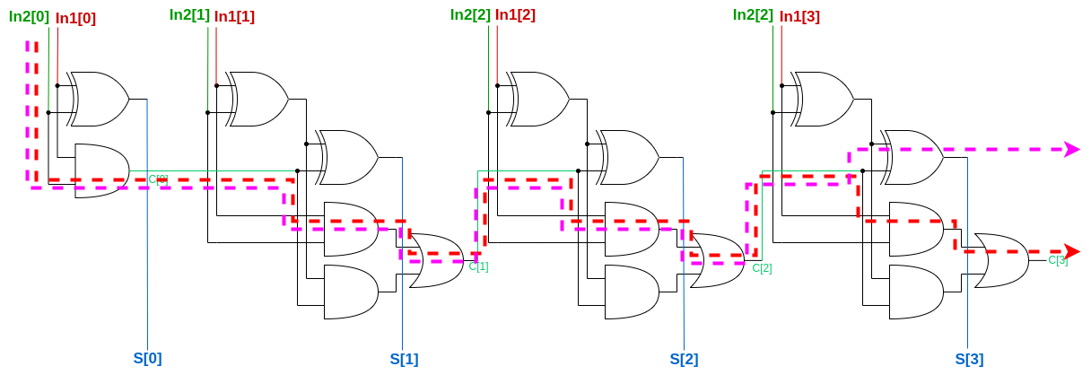
Propagation delay is a term used to indicate the time required by a single logic gate or a complex combinational circuit, consisting of thousands of gates, to achieve a stable output after a change in the input. This delay is always calculated considering the worst-case scenario, where a flip of an input bit propagates through the entire structure of the circuit to the output; in the image above, the circuit propagation delay is represented by the interval between the clock rising edge (when the input - ideally - changes) to the time when the output is correct and available to the next memory element. As you can see, the output of the combinational logic could be stable at different times after the input is applied, depending on the type of input and the path of each signal: if the propagation delay is too high, output could be stable when the next clock edge arrives, violating hold and setup times, invalidating thus the circuit!
This quantity, related to a combinational logic circuit, is fundamental to estimating the time required to complete an operation.
Propagation delay is typically measured when signals are at 50% of their output final voltage, as shown in the figure.
Propagation delay poses a limit to the maximum clock frequency of the digital circuit. $$\frac{1}{f_{clk}} = T_{clk} \gt max(t_{pd,i-j})$$ being $$t_{pd} = t_{out@50\%} - t_{in@50\%}$$ 'i-j' is a generic path from input 'i' to output 'j'.
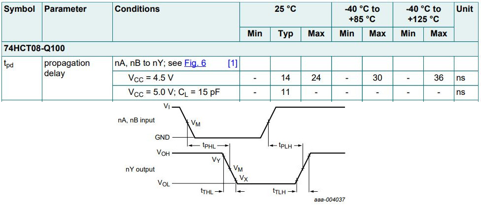
Just to give you an idea of a real tpd value and measurement, take a look at this AND gate made by NEXPERIA.
Rise and fall times
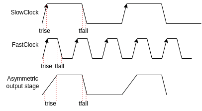
These quantities are related to the physical properties of gates or memory elements used in the design rather than the whole combinational or sequential block. Typically, rise and fall times are way shorter than propagation delay, but, when the clock frequency becomes very high, they are not negligible anymore: you must always consider them when you analyse the delay from one point to another one.
Rise and fall times are used to describe the behaviour of the output stage of both sequential and combinational circuits; they are typically expressed as the time needed by the output of a digital component to go from 10% to 90% (Low-to-High transition) of its output voltage and vice versa (High-to-Low transition). Note that, depending on the output topology and its physical design, 10%-to-90% rise time may differ from 90%-to-10% fall time. $$t_{r} = t_{x(t)@90\%} - t_{x(t)@10\%}$$ $$t_{f} = t_{x(t)@10\%} - t_{x(t)@90\%}$$ where x is a generic signal
Take a look at rise and fall times of the NEXPERIA 74HCT08-Q100, the same component as above.

Setup time
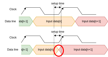
In sequential circuits, the input of a memory element must be stable for some time before the clock edge event: this amount of time is called 'setup time' and, if it is violated, the memory element could store a wrong value. You must NEVER violate a setup time when designing a digital application.
Hold time

In sequential circuits, the hold time is the amount of time, starting from the clock edge, during which the data at the input of a memory element should be stable to ensure correct data storage. Again, if this time is violated, the memory element could retain a wrong value at its output.
Skew

We considered the clock as a very fast, sharp edge, accurate signal, equally distributed through the whole design. However, in very large designs, where the die area is pretty large and all the subunits must work at the same clock frequency, this signal must reach areas, far away from the source, generating a delay that must be considered. Skew is, generically, the difference of time between the clock edge arrival to a point of a circuit and another one, caused mainly by the parasitic elements of the interconnections (clock interconnection capacitance overall). To avoid the problem shown by the red line in the image above, there are some parts of the circuit, added to the design, to restore the clock so that a single output driving the clock signal sees a lower capacitance, edges are sharper and delay among the subunits is reduced. $$t_{sk} = t_{x(t),A} - t_{x(t),B}$$ where x is a generic signal and A and B are two different points of the circuit where x signal propagates.
Jitter

Another clock non-ideality is the so-called jitter. We previously said that clock signals are always fixed frequency and duty cycle square waves; however, the edges of this sync signal continuously change with respect to the instant where they should be. The difference between the instant when the ideal edge should be and when the edge arrives is called jitter. It is typically measured considering the instant when the clock signal is at 50% of its final voltage.
Share this page


Comments
Be polite and respectful in the comments section. In case of doubts, read this before posting.
Posted comments ⮧
Comment section still empty.
INDEX
INFO
STATISTICS
PREVIOUS ARTICLE
NEXT ARTICLE
CONTACTS
SHARE