➔ Index of ⦁ Buck Converter ⦁
Buck converter - Closing the loop
Compensation strategies for a voltage-controlled (VCM) buck converter operating in CCM
Need for feedback!
The feedback network of a voltage-controlled CCM buck converter is essentially a resistor divider connected to the input of an error amplifier that compares it with a reference value. The output (an error voltage) is sent to a PWM modulator, which generates the required pulse to be connected to the gate of the high-side MOSFET.
However, before going on, let's see why we need a specifically designed feedback and why this network must have some specific characteristics and transfer function: let's assume that the controller is just a block with unitary gain, so no compensation is done, and the feedback voltage is the output voltage itself, with no voltage divider in the middle. $$\begin{cases} G_{vd} = \frac{V_I}{s^2 LC + s \frac{L}{R} + 1} \quad Duty-to-Output \\ G_{dc} = \frac{1}{V_{ramp,pk}} \quad Control-to-Duty \\ G_c = 1 \quad Controller \\ G_{fb} = 1 \quad Feedback \ network \end{cases}$$ The open loop transfer function T is $$T = G_{vd}G_{dc}G_{c}G_{fb} = \frac{V_I}{s^2 LC + s \frac{L}{R} + 1} \cdot \frac{1}{V_{ramp,pk}} \cdot 1 \cdot 1$$ Now, I need some numerical values to plot the T transfer function on a Bode plot: $$L = 10 \mu H$$ $$DCR = 30mOhm$$ $$C = 200 \mu F$$ $$ESR = 1 mOhm$$ $$R_L = 100$$ $$V_{ramp,pk} = 1V$$ $$V_{ref} = V_{o,target} = 1.8V$$ $$V_g = 5V$$ The open loop transfer function is shown in the image below: note the very low phase margin, around 4° at a crossover frequency of 9kHz circa! Well, I think that this is enough to justify the need for a compensation network in the feedback branch :)
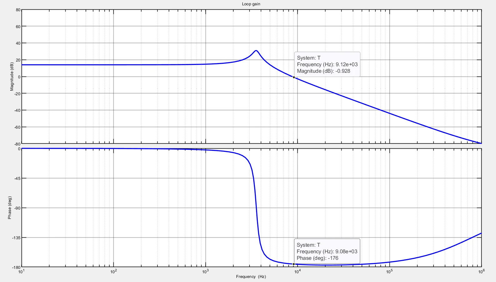
The DC gain of the open loop transfer function has a fixed value: this is not the best behaviour since we need a T whose gain at s=0 is as high as possible, ideally infinite, so that the overall closed loop gain is determined by the feedback circuit only. The have such a beahviour, we need a pole in s=0, added through a proper compensation circuit.
Compensation
To provide stability to the control loop, we need a compensating network, to be added around the error amplifier.
I'll not go into the details of error amplifier and compensation networks design here; I'm just using a 3rd type compensator (two zeros and three poles) for voltage mode buck converter operating in CCM: remember that this is the right compensator for this kind of converter, type I and II are not suitable since the required phase boost is quite high. $$ G_c = G_{cm} \frac{(1+\frac{\omega_{z1}}{s})(1+\frac{s}{\omega_{z2}})}{(1+\frac{s}{\omega_{p1}})(1+\frac{s}{\omega_{p2}})} $$ Let's find a formula for that 3rd type compensator considering the passive components around the opamp: $$ Gc = \frac{1}{(sR_{s2}(C_{f1}+C_{f2}))} \cdot \frac{(sC_{f1}R_{f1}+1)}{(sR_{f1}\frac{C_{f1}C_{f2}}{C_{f1}+C_{f2}}+1)} \cdot \frac{(sC_{s1}(R_{s1}+R_{s2})+1)}{(sC_{s1}R_{s1}+1)} $$
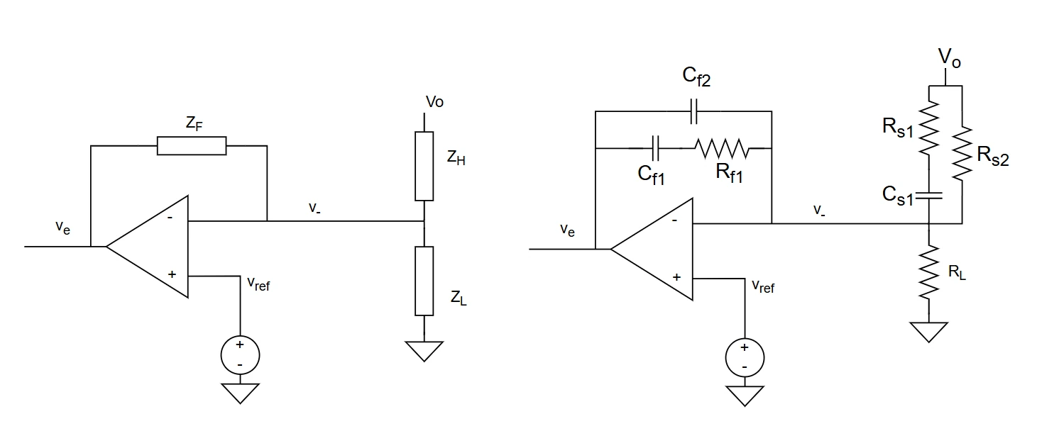
Adding the compensator to the loop function, we can get a response, boosting the phase were is is required and eventually managing the DC gain. The values used for this example are listed here $$G_{cm} = 1$$ $$\omega_{z1} = 2\pi 3e3 \ rad/s$$ $$\omega_{z2} = 2\pi 1e3 \ rad/s$$ $$\omega_{p1} = 2\pi 100e3 \ rad/s$$ $$\omega_{p2} = 2\pi 1e6 \ rad/s$$
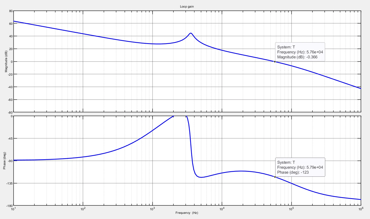
As you can see, the VMC CCM buck converter has that double pole that must be compensated through a sufficient phase boost: in the final Bode plot we still see the disruptive effect of that conjugated complex double pole; we will see how a current controlled buck, and in general a current controlled DCDC, gives many more advantages for stability and compensation with respect to a simple voltage mode DCDC.
Navigate
Share this page


Comments
Be polite and respectful in the comments section. In case of doubts, read this before posting.
Posted comments ⮧
Comment section still empty.
INDEX
INFO
STATISTICS
PREVIOUS ARTICLE
CONTACTS
SHARE